Recently I began a hobby project to recreate a 1980s IBM XT personal computer using a mix of authentic parts and modern technology. I had a clear goal in mind: I wanted to be able to play the EGA version of Monkey Island 1 on it, with no features missing. This means I need mouse support, a hard drive with write access to game saves, and adlib audio, my favorite version of the game’s musical score.
The catalyst for this project was the discovery that there are low-power versions of the NEC V20 CPU (UPD70108H) available, which is compatible with the Intel 8088 used in the XT. Being a low-power version, it simplifies connection to the FPGA, which typically works with a 3.3-volt IO voltage. The XT was coupled with a low-power 1MB SRAM chip (CY62158EV30) to provide its 640KB of memory, and I started working on the bones of a complete system.
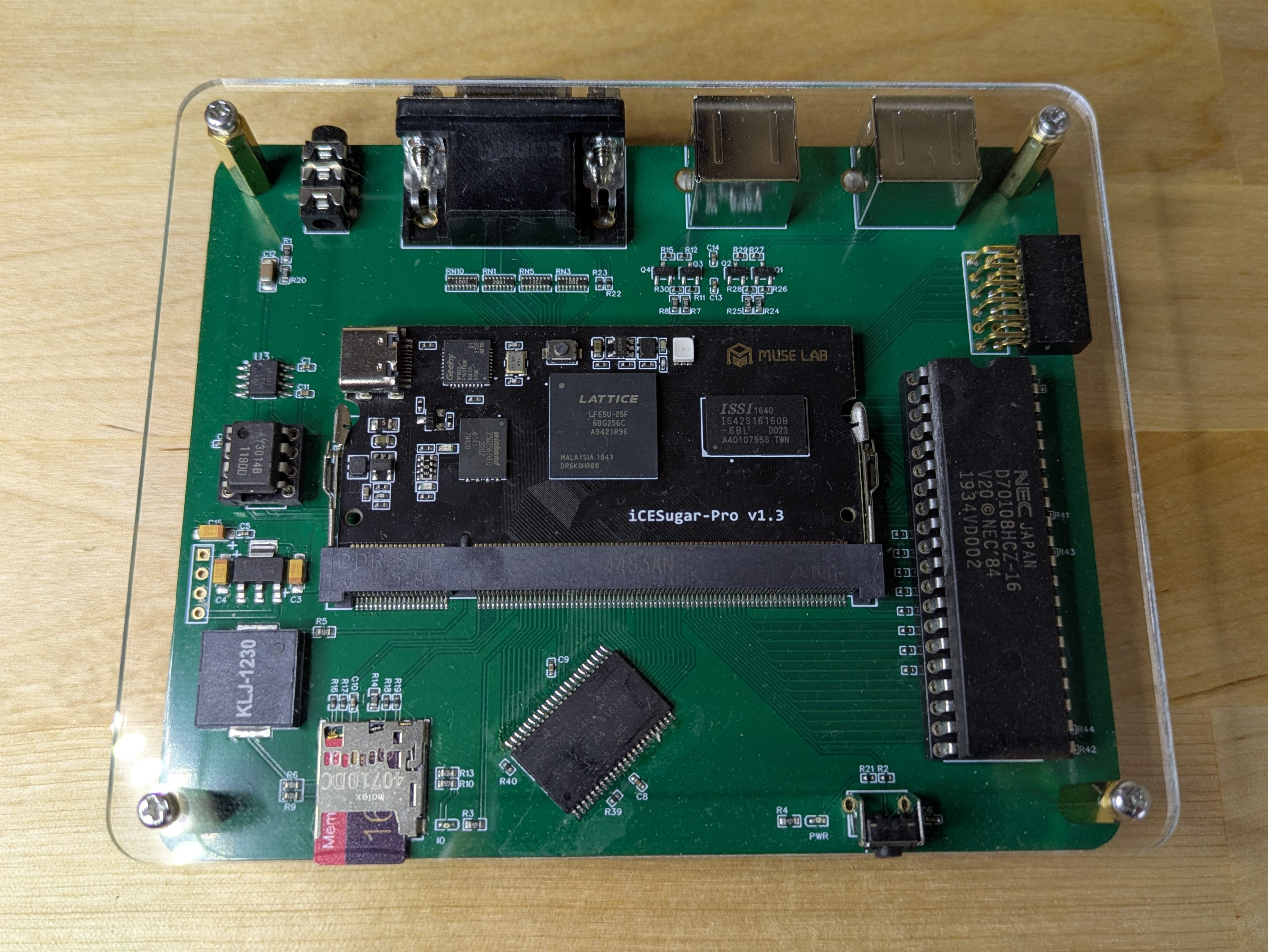
I started by designing the hardware of the system, which would serve as my development board while I worked on the software/gateware. The following features were added:
– DIP-40 socket for low-power NEC V20 CPUs
– 1MB SRAM chip for system memory
– An IceSugar-Pro FPGA board with the Lattice LFE5U-25F
-Dual PS/2 connectors for keyboard and mouse
– Micro SD card socket to act as a fixed disk
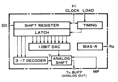
– An authentic YM3014B digital-to-analog converter for audio
– A piezo speaker that can be operated by a programmable-interval-timer for system blips
– Finally, a reset switch and some status LEDs

I created my design using EasyEDA CAD software because I’m already familiar with it, and it has a really nice integration with the JLCPCB PCB assembly service. Some components of the design are so complex that it is difficult for me to solder them alone. However, after the board arrived I had to solder the SRAM chips as they were not stocked by LCSC so I had to get them from elsewhere.

The first step was to write a bus controller for the processor. The V20 CPU clock is more forgiving than the original i8088 as it can be run down to 0hz and uses the regular 50% duty cycle. The external interface to the 8088 CPU operates in terms of bus cycles. Just at the beginning of the cycle the CPU sets up some pins to tell everyone what it wants to do… read memory, write to IO, etc. Each type of bus cycle follows a specific sequence of events occurring over several clock cycles. It was straight forward to creating a state machine that could detect the start of a bus-cycle, figure out what type it was, and then produce or consume data as needed by the CPU. The key here, was to ensure that all timing requirements were met, so that the signals generated by the CPU were sampled at the correct time, and the signals required by the CPU were correctly conducted before they were read by the CPU.

My first test for the bus controller was to write a simple program to execute on the V20 using NASM, with a simple goal… it would flash an LED mapped to an IO port address. Simple, but a flashing LED appears to be the hardware equivalent of a software hello-world. For the initial version, the program was simply loaded into the FPGA block RAM and used directly as system memory.
Later, I used a more complex approach to memory access. For example, the BIOS is loaded into the FPGA block RAM, so that CPU memory reads come from that instead of the system SRAM chip. Video memory is still implemented in a different way. CPU memory writes are passed to both video memory block RAM and system SRAM, but CPU reads always come from system SRAM only. This means that I have an additional read port on the video block RAM that can be used by the VGA signal generator to display the video memory contents.
After my success with the Blinky program, I installed a virtual copy of the Supersoft/Landmark diagnostic ROM in place of the BIOS and wrote a basic CGA adapter for video output. I was then able to use the diagnostic ROM to test the SRAM memory interface as well as some peripherals required for the XT such as the Programmable-Interval-Timer (i8253) and the Programmable-Interrupt-Controller (i8259).
Once I was confident the basic system was stable I swapped in a generic XT BIOS from https://www.phatcode.net in place of the diagnostic ROM. It was amazing to see the BIOS boot and complain about not finding a boot disk.
Fixed disk access is achieved by making a small Verilog SPI controller accessible to the CPU through some unused IO ports. I then wrote an option ROM to handle the BIOS INT13H (disk service) calls, which had routines that could issue commands to the SD-card over SPI. The difficult part for me was learning the SD card protocol and then writing 8088 assembly to perform the correct operations. The mapping itself is pretty straightforward as both the SD card and DOS assume 512byte sectors.
I saved a lot of time when writing the option ROM by developing and debugging the code using the board’s software emulator, which I cobbled together. Some historical sources for this can be found here: https://github.com/bit-hack/iceXt/tree/master/misc/emulator
Perhaps the hardest part of the project, surprisingly, was getting the mouse to work. Mice from the XT era will usually be connected to a UART serial port. However I did put a PS/2 connector on the hardware board, and those mice use a very different protocol. In my efforts to support the mouse I began learning about PS/2 devices, however I would need to implement a more complex keyboard controller, and the BIOS also lacked support for such modern peripherals, and I didn’t quite feel like I understood everything I needed to make it work.
What makes this tricky is that PS/2 is a bidirectional protocol, and the PC has to ask the mouse to transmit updates, otherwise we wouldn’t receive any. This added more complexity than I wanted. On the other hand, it is relatively easy to work with the keyboard and send keypresses without asking.
I chose an option. I wrote some Verilog code to talk directly to the PS/2 mouse, telling it to start sending mouse events as early as the boot process would require. When the bridge receives mouse events, it translates them through the pseudo-UART peripheral and presents them to the computer. I implemented a basic PS/2 mouse in a serial mouse bridge. A bit complicated but it works really well.
During this process, I lobotomized a spare mouse by adding a logic analyzer clk and dat pads inside the mouse. I was then able to capture the communication between a real PC and the mouse and observe it during use. This gave me invaluable insight into how the protocol works, and what to expect from a real mouse.
I also found that having real waveforms to see made it much easier to test components of my design in Verilator, a Verilog simulator, because I could closely model the excitation I would see when running it in the FPGA.

Like the XT, one of the PIT timer’s channels is used to drive the internal speaker to produce the bleep and bloop sounds. I enhanced this by triggering short pulses triggering disk access from a piezo speaker as a crude simulation of a hard disk seek. I think it really adds to the experience when you can hear your computer thinking while it’s performing its tasks. However, when it comes to music, the internal PC speaker quickly loses its charm. Writing a YM3812 implementation (the FM chip used in the Adlib card) is beyond my skill level, but thankfully Jose Tejada has written a wonderful open source version that I was able to incorporate into my project; https://github.com/jotego/jtopl.
I wrote a small Verilog module to take the PCM sample data generated by this soft YM3812 and convert it to the unusual 3:10 floating point format required by the YM3014 DAC on my board. This is similar to the operation of real Adlib hardware, where the YM3812 generates serial audio data and sends it to the YM3014 DAC chip. A modern I2S DAC might be neat, but the chance to play with an authentic DAC seemed a little more fun to me. The combined result of all this is the same beautiful crisp FM tone that I loved when I played games on my PC growing up.

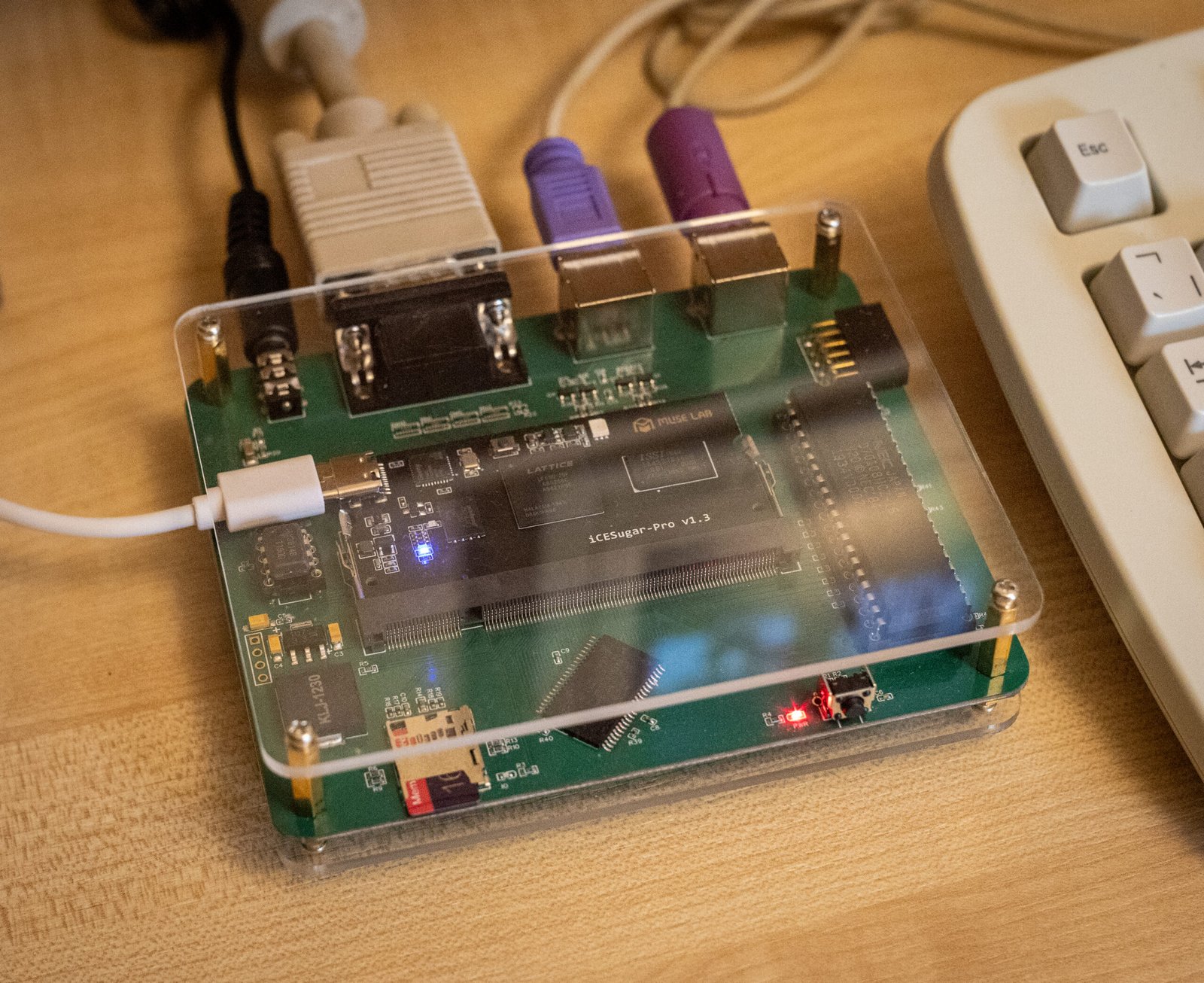
Many other elements of this project have been hidden or omitted, such as support for CGA and EGA graphics. There’s even a USB to UART bridge for sending files directly from the host PC to the SD card. I also made some nice clear acrylic panels on the CNC machine to complete the design and protect the bare PCB.

A video demo is shown below.
Unfortunately the phase difference between the monitor and my camera is causing a lot of screen tearing. It is not directly visible.
Source code, schematics and Gerber files are available on Github here: https://github.com/bit-hack/iceXt
Thanks for reading!
